
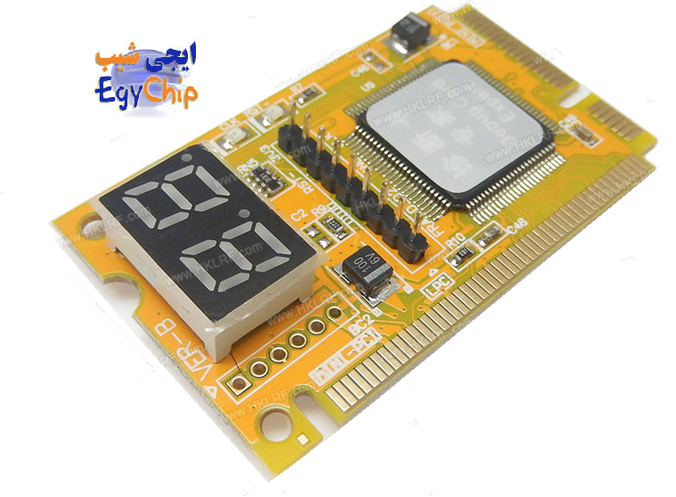
3 in 1 Mini PCI-E PCI LPC 2 Digit PC Analyzer Combo-Debug-Card repair tool
Mini PCI/Mini PCI-E/LPC Combo-Debug-Card VIP version Notebook Combo-Debug-Card (VIP Version) User Guide
This notebook Combo-Debug Card Uses 4-layers PCB design to provide a very stable signal quality. Also, it uses Tantalum capacitance to provide good power supply. So this VIP version Debug card is more suitable to be used in poor environment. This VIP version is the upgraded version of the Combo-Debug-Card, and it supports three bus interfaces: MINI PCI, MINI PCI-E and LPC. This product is easy to use, and is designed with good stability. It is your ideal tool for notebook repair.
combo –debug- card structure and usage
- Mini-PCI interface:
This is used to connect this Combo Debug Card to notebook’s Mini-PCI slot. - Mini-PCI-E interface:
This is used to connect this Combo Debug Card to notebook’s Mini-PCI-e slot - LPC interface:
This is used to connect this Combo Debug Card to notebook’s LPC connector. - ASIC
- Two 7-segment LEDS:
This is used to display the Error-code - Test port:
This port is reserved, and end-user should not use this port. - indicator : this is for showing the status of CLK and RST signal.
The Mini-PCI interface in the Combo-Debug-Card
Mini PCI is a general interface, which is used in notebook. It includes 124 pins. This combo-debug-card doesn’t fully use those pins, and only 101 pins are used. When installing this combo-debug-card to your notebook main-board , you will find the combo-debug-card is shorter than the notebook Mini-PCI slot. This is correct, and it servers better for you to plug or unplug this combo-debug-card.
The Mini-PCI-e interface in the Combo-Debug-Card
Mini-PCI is used as a trend in the new notebooks. Comparing to Mini-PCI, Mini-PCI-e occupies less space. This Combo-Debug-Card doesn’t use all of the Mini-PCI-e bus pins. And only the below pins are used: PIN-8, PIN-10, PIN-12, PIN-14, PIN-16, PIN-17, and PIN-19. in the Mini-PCI-e spec, those pins are reserved, and it is not standard, so some of Notebook manufacturers define it as a LPC debug-port. And more and more notebook manufacturers are using this standard, such as IBM, Toshiba, HP, ASUS, TCL and etc……this Combo-Debug-Card can only work in the notebooks, which are with the LPC debug-port definition. For the notebooks, which don’t support this LPC debug-port definition, this Combo-debug-card PCI-E interface will not work.
Note: Please be aware that Mini-PCI-e is supported with limitation, and it can works in most of notebooks, but not all.
The LPC interface in the Combo-Debug-Card
For the user, whose notebooks don’t support the Mini-PCI interface and the Mini-PCI-e interface, you can use the third port: LPC interface. LPC interface exists in all notebook main-boards. In the Combo-Debug-Card, from left to right, the LPC definition is:
PIN1-LFRAME﹟, PIN2-LAD3, PIN3-LAD2, PIN4-LAD1, PIN5-LAD0, PIN6-GND, PIN7-LRESET﹟, PIN8- LCLK, PIN9-3.3V
Usually, the notebook boards haven’t LPC connectors or slots. And the users will need to connect this LPC port to the notebook by using wires. Below is some description for how to connect the Combo-Debug-Card to your notebook through this LPC interface.
If your notebooks use LPC VBIOS, you can connect the Combo-Debug-Card to your notebook’s VBIOS bus.
LPC VBIOS Pin definition:
PIN2-RST﹟ PIN13-LAD0 PIN14-LAD1 PIN15-LAD2 PIN16-GND PIN17-LAD3 PIN23-LFRAME﹟ PIN25-VCC PIN31-CLK
You can connect this Combo-Debug-Card to any LPC bus. Some LPC interface chips are listed as below. You can connect the Combo-Debug-Card to the corresponding pins. For more information, please refer those chip’s datasheets.
Note: this Combo-Debug-Card uses 3.3V as power supply, and you can use any 3V3 and GND signals in your notebook main-board. Please be aware that connecting the Combo-Debug-Card to a non-3.3V power may damage this Combo-Debug-Card.
For IBM X 60 notebooks, the LPC interfaces are located in the U39 slot of the main-board. The Pin definitions are as below: A2->LRESET﹟ A3->LFRAME﹟ A5->LCLK A9->LAD3 A10->LAD2 A11->LAD1 A12->LAD0
For IBM T6 R6 notebooks, the LPC interfaces are located in the J26 slot of the main-board. The Pin definitions are as below: A1->LCLK, A3->LFRAME﹟ B2->LRESET﹟ B7->LAD3 A7->LAD2 B6->LAD1 A6->LAD0
The LED-Display in the Combo-Debug-Card
The Display includes Error-Code display, Bus-Type display, and “CLK”,”RST” signal, status display .
1, Error-Code display: It is composed with two 7-segment LED s.
2, Bus-Type display: The two “Dots” of the LED s are used to indicate the notebook bus type. The left side “Dot” is for Mini-PCI bus, and the right side “Dot” is for Mini-PCI-e and LPC bus. When the notebook works in Mini-PCI bus, the right side “Dot” will be lighted.
3, “CLK”, “RST” signal status display: when you hold on the notebook’s “RESET” button, the “RST” indicator will be lighted, and the “CLK” indicator will be off. When you release the notebook “RESET” button, the “RST” indicator will be off, and the “CLK” indicator will be twinkled.
Part of Error-Code explanation
When the notebooks are running, this Combo-Debug-Card will show the corresponding debug code. If there is a problem in the notebook, you can judge the problem by the debug code. Below is the explanation for some main error codes.
AWARD BIOS:The explanation when the Combo-Debug-Card shows the below debug codes.
Code Explanation
C0 Close cache
01 Processor test
07 CMOS test
C1 Memory size test
0A Set the interrupt table
0C Initiate the keyboard
0D Initiate the Graphic card
1A Show CPU frequency
3C CMOS setting
42 Initiate hardware
52 Test the extended ROM
FF Boot AMI BIOS: The explanation when the Combo-Debug-Card shows the below debug codes.
Code Explanation
00 Error in self test
01 Error in processor test
0D,0F Error in CMOS test
1A~22 Error in Memory test
3A Error in graphic card
FF Pass the self test Q/A
Question: “RST” indicator is off, but “CLK” indicator is NOT twinkled.
Answer: this symptom shows there is no CLK signal for debug card so that the “CLK” indicator isn’t twinkled .Usually, it may mean the motherboard can NOT support this Mini-PCI-e interface. Please use Mini-PCI or LPC interface to test it.
Question: “RST” indicator is off ,and “CLK” indicator is twinkled. But it shows “00”
Answer: In this case, please check the Bus-Type display to check if the Bus-Type display is corresponding to the bus type.

